Skip links

VLSI Projects

VLSI projects | VHDL Verilog VLSI projects
bangalore INDIA

Innowitech Solutions bangalore offers VLSI projects guidance. It offers VLSI projects developed using VHDL or Verilog e.g. IFFT FFT core, OFDM, LDACS, DPWM for DC-DC converter, MIPS architecture etc. in Bangalore,INDIA.

Following table mentions list of VLSI projects offered using VHDL/Verilog by Innowitech Solutions Bangalore, INDIA.

Pipelined IFFT FFT IP Core

This page covers VLSI project on Pipelined IFFT and FFT IP cores. This VLSI project on Pipelined IFFT/FFT is implemented in Verilog.This VLSI project is guided by Innowitech,Bangalore,INDIA.

The FFT is one of the most widely used algorithms for calculating the Discrete Fourier Transform (DFT) owing to its efficiency in reducing computation time. Fast Fourier Transform (FFT) has been used in a wide range of applications, such as wide-band mobile digital communication system based on Orthogonal Frequency Division Multiplexing (OFDM) principle, where the system implementation is only feasible when the equipment complexity and power consumption are greatly reduced by utilizing a real-time FFT transformer to replace the bank of (de)modulators for each individual sub-carriers.FFT, as an efficient algorithm to compute the Discrete Fourier Transform (DFT), is one of the most important operations in modern digital signal Processing and communication systems.

The design of FFT is carried out in MATLAB and verified. RTL coding is done using Verilog HDL, Xilinx Spartan 3A FPGA will be used for implementation. Modelsim is used for simulation Functional and Timing simulations.

Software Tools: Xilinx ISE, MATLAB, Modelsim, Active HDL
Languages: Verilog HDL, MATLAB

OFDM Transmitter OFDM Receiver IP Core

This page covers VLSI project on OFDM Transmitter and OFDM Receiver. This VLSI project on OFDM Transmitter and Receiver is implemented in Verilog.This VLSI project is guided by Innowitech,Bangalore,INDIA.

The design of OFDM physical Layer Transmitter and Receiver will be carried out in MATLAB and verified .Transmitter chain blocks will be done in Verilog-HDL and will be generating the IQ data vector which will be compared with MATLAB prove the design, The above diagram describes the baseband OFDM transmitter chain.

Languages Used: Verilog HDL, MATLAB
Tools: Xilinx ISE, Modelsim, Active HDL, MATLAB-SIMULINK

LDACS Physical layer

The MATLAB and corresponsing Verilog implementation of LDACS-1 and LDACS-2 Physical layer.

DWDM technique for DC to DC converter

This page covers VLSI project on DWDM technique for DC to DC converter. This VLSI project on DC to DC converter is implemented in Verilog. This VLSI project is guided by Innowitech,Bangalore,INDIA.

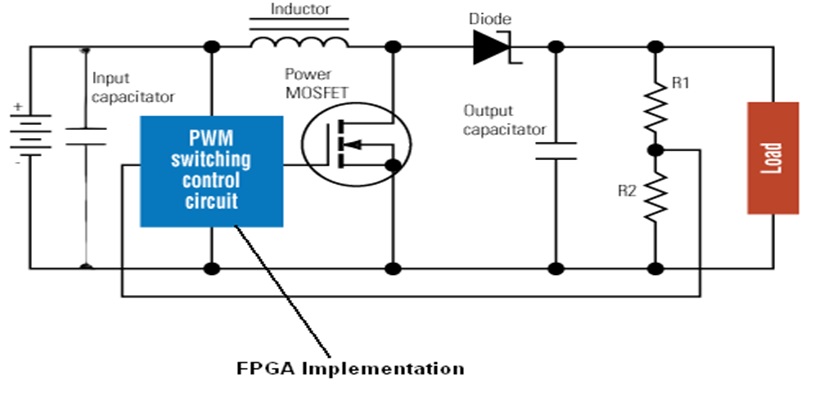
Project Objective: Switching control Circuit is the common block for Buck and Boost convertors above, our main focus of implementation is design of FPGA based Digital controller for a DC-DC convertor for Soc. The output voltage of a DC-DC convertor depends on the Switching control circuit (FPGA Digital controller-PWM). Hence our focus is to design a FPGA based Digital controller.

Buck and Boost convertor models will be first developed in MATLAB-SIMULINK, which will be based on PWM block. Verilog HDL coding will be done for the Digital Controller, synthesis will be done using Xilinx ISE, and Behavioral and Timing simulation will be done using Modelsim/Xilinx Simulator/Active HDL. After verification of code it will be downloaded onto a Spartan 3AN FPGA board. The pulse width output can be verified by an Oscilloscope and building an Analog Buck or Boost convertor circuit and connecting it to the FPGA Pin.

Tools: Xilinx ISE, Modelsim, Active HDL, MATLAB-SIMULINK
Hardware: FPGA Board, Buck Circuit, Oscilloscope

MIPS Architecture Implementation

This page covers VLSI project on MIPS Architecture implementation. This VLSI project on MIPS Architecture is implemented in Verilog.This VLSI project is guided by Innowitech,Bangalore,INDIA.

This Projects aims at HDL development/Implementation of a MIPS Processor, which supports MIPS Instruction Sub Set, which covers R-Type, I-type and J type Instruction. The architecture of MIPS is thoroughly studies and analyzed. Each Block is coded in Verilog HDL, and then verified. In a similar manner all the blocks of the MIPS system are coded and tested. After this stage all the blocks are integrated to form the MIPS Data Path and Instruction path. We can write a Program, convert it to Opcode, store the Opcode in memory and execute the code and to verify if the Program is working as expected. Once Verilog HDL code is complete, Simulations and synthesis will be done.

Following are tools which will be used:
Tools: Xilinx ISE, Model Sim, Active HDL
Language: Verilog HDL

Other VLSI Projects

We can take up any other VLSI projects also after studying the requirements. So write to us with specific details.

Innowitech Institute offer VLSI projects in Bangalore at their facility located in RT Nagar as per student’s choice of language either VHDL or Verilog. Innowitech offers VLSI projects in other domain areas which are not specified on this page. So write to us with your specific need at enquiry@innowitech.com.

About Bangalore,INDIA

Bangalore is well-known as silicon valley of India due to its position as leading IT exporter. Today Bangalore is home to most well recognized colleges, research institutes in INDIA. Numerous software technology companies, public sector undertakings, wireless, telecom, aerospace and defense organizations are located in the bangalore city.